HDLBits答案(12)_Verilog移位寄存器
Verilog移位寄存器
前言
今天更新一节寄存器相关内容,其中涉及CRC校验的内容是用线性反馈移位寄存器搭建而成的。
基础知识介绍
什么是移位寄存器?
移位寄存器(Shift Register)是一种特殊的寄存器,它能够在时钟脉冲的作用下,将存储的数据向左或向右移动一位或多位。
生活中的类比:
想象一排人站成一队,每个人手里拿着一个球(代表数据0或1)。当听到”移位”的命令时:
- 每个人把手里的球传给旁边的人
- 最边上的人要么把球传出去(丢弃),要么从外面接收一个新球
这就是移位寄存器的工作原理!
移位寄存器的分类
按移位方向分:
- 左移寄存器:数据向左移动
- 右移寄存器:数据向右移动
- 双向移位寄存器:既可以左移也可以右移
按输入输出方式分:
- 串行输入串行输出(SISO)
- 串行输入并行输出(SIPO)
- 并行输入串行输出(PISO)
- 并行输入并行输出(PIPO)
特殊类型:
- 循环移位寄存器:移出的数据从另一端移回来
- 算术移位寄存器:保持符号位不变
- 线性反馈移位寄存器(LFSR):用于产生伪随机序列
为什么需要移位寄存器?
移位寄存器在数字系统中有很多应用:
- 数据传输:串并转换(串行数据转并行数据)
- 时序控制:产生特定的时序序列
- CRC校验:通信中常用的检错码
- 伪随机数生成:LFSR可以产生近似随机的序列
- 数据缓冲:临时存储和调整数据流
入门者避坑指南
在设计移位寄存器时,初学者很容易犯一些常见的错误,下面我们来总结一下。
错误1:移位方向搞反
错误表现:1
2// ❌ 错误示例:想要右移,结果写成了左移
q <= {q[2:0], 1'b0}; // 这是左移!不是右移!
错误原因分析:
在Verilog中,移位的方向取决于你如何拼接位:
- 左移:低位补0,高位丢弃 →
{q[2:0], 1'b0} - 右移:高位补0,低位丢弃 →
{1'b0, q[3:1]}
正确做法对比:1
2
3
4
5// ✅ 正确示例:右移
q <= {1'b0, q[3:1]};
// ✅ 正确示例:左移
q <= {q[2:0], 1'b0};
错误2:拼接操作符的顺序错误
错误表现:1
2// ❌ 错误示例:拼接顺序搞反了
q <= {q[0], q[3:1]}; // 想要循环右移,但顺序错了
错误原因分析:
在拼接操作符 {} 中,信号的顺序是从左到右对应高位到低位。对于循环右移,应该是把最低位移到最高位。
正确做法对比:1
2
3
4
5// ✅ 正确示例:循环右移
q <= {q[0], q[3:1]}; // 最低位q[0]变成新的最高位
// ✅ 正确示例:循环左移
q <= {q[2:0], q[3]}; // 最高位q[3]变成新的最低位
错误3:算术移位时没有保持符号位
错误表现:1
2// ❌ 错误示例:算术右移时没有正确处理符号位
q <= {1'b0, q[63:1]}; // 对于负数,符号位应该保持为1!
错误原因分析:
对于有符号数的算术右移,符号位(最高位)应该保持不变,而不是简单地补0!
正确做法对比:1
2
3
4
5// ✅ 正确示例:算术右移(保持符号位)
q <= {q[63], q[63:1]}; // 符号位q[63]保持不变
// ✅ 正确示例:算术右移8位
q <= {{8{q[63]}}, q[63:8]}; // 复制8次符号位
题库
题目描述1:
构建一个4bit的移位寄存器(右移),含异步复位、同步加载和使能。
- areset:让寄存器复位为0
- load:加载4bit数据到移位寄存器中,不移位
- ena:使能右移
- q:移位寄存器中的内容
Solution1:
1 | module top_module( |
题目描述2:
构建一个100位的左右旋转器,同步load,左右旋转需使能。旋转器从另一端输入移位的位元,不像移位器那样丢弃移位出的位元而以零位移位。如果启用,旋转器就会旋转这些位,而不会修改或丢弃它们。
- load:加载100位的移位寄存器数据
- ena[1:0]:2’b01 右转1bit; 2’b10 左转1bit;其他情况不转
- q:旋转器内容
Solution2:
1 | module top_module( |
题目描述3:
建立一个64位算术移位寄存器,同步加载。移位器可以左右移位,并按数量选择1位或8位的移位。
- load:加载数据
- ena:决定是否移位
- amount:决定移位方向与数量:2’b00:左移1位;2’b01:左移8位;2’b10:右移1位;2’b11:右移8位
- q:寄存器内容(输出)
Solution3:
1 | module top_module( |
题目描述4:
构造线性移位寄存器,reset应当使LFSR归1。
Solution4:
1 | module top_module( |
题目描述5:
为这个序列电路编写Verilog代码。假设你要在DE1-SoC板上实现这个电路。将R输入连接到SW开关,将时钟连接到密钥[0],将L连接到密钥[1],将Q输出连接到红灯LEDR上。
Solution5:
1 | module top_module ( |
题目描述6:
构建一个32位的Galois LFSR,其taps位置为32、22、2和1。
Solution6:
1 | module top_module( |
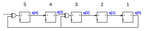
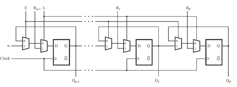
题目描述7:实现如下电路图
Solution7:
1 | module top_module ( |
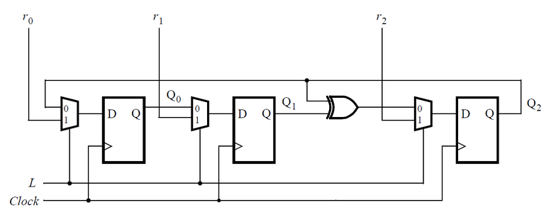
题目描述8:实现如下电路图
- Connect the R inputs to the SW switches,
- clk to KEY[0],
- E to KEY[1],
- L to KEY[2], and
- w to KEY[3].
- Connect the outputs to the red lights LEDR[3:0].
Solution8:
1 | module top_module ( |
题目描述9:
在这个问题中,你将为一个8x1存储器设计一个电路,在这个电路中,写入到存储器是通过移位来完成的,而读取是”随机访问”,就像在一个典型的RAM中一样。然后您将使用该电路实现一个3输入逻辑功能。
首先,用8个d类型触发器创建一个8位移位寄存器。标记为Q[0]到Q[7]。移位寄存器输入称为S,输入Q[0] (MSB先移位)。使能输入enable控制是否移位,扩展电路使其有3个额外的输入A,B,C和一个输出Z。电路的行为应该如下:当ABC为000时,Z=Q[0],当ABC为001时,Z=Q[1],以此类推。你的电路应该只包含8位移位寄存器和多路复用器。这个电路称为3输入查找表(LUT)。
Solution9:
1 | module top_module ( |
小结
今天更新了移位寄存器部分的答案,注意最后一题用了一些技巧来简化代码书写,但实现时电路并无差异,体现了HDL中”Describe”的特性。
 微信
微信 支付宝
支付宝