HDLBits答案(3)_Verilog模块的例化与调用
HDLBits_Verilog模块的例化与调用
模块
如果把单个逻辑门比作电子元件,那么模块就可以理解为一块电路板。它把多个元件封装在一起,对外只留下一些接口(端口),这样我们就可以通过连接这些接口来构建更复杂的系统。
在Verilog中,只要所有模块都属于同一个项目,就可以通过在一个模块内部实例化另一个模块来创建层次结构。但要注意:一个模块的代码不能写在另一个模块的主体中——也就是说,模块之间是平级关系,不是嵌套关系。
打个比方,你可以把主板插在电脑机箱里,但你不能把主板的电路图直接画在机箱的电路图里面,它们是分开设计的。
模块连接的两种方式
有两种常见的方式将wire信号连接到模块端口上:
1. 按位置连接
1 | mod_a instance1 (wa, wb, wc); |
就像老式的耳机插头,插针的顺序是固定的,第一个位置对应第一个信号,第二个位置对应第二个信号……
2. 按名称连接
1 | mod_a instance2 (.out(wc), .in1(wa), .in2(wb)); |
这就像USB Type-C接口,不管你怎么插,只要名称对应就能连接。.端口名(连接信号)这种格式清晰地表达了连接关系。
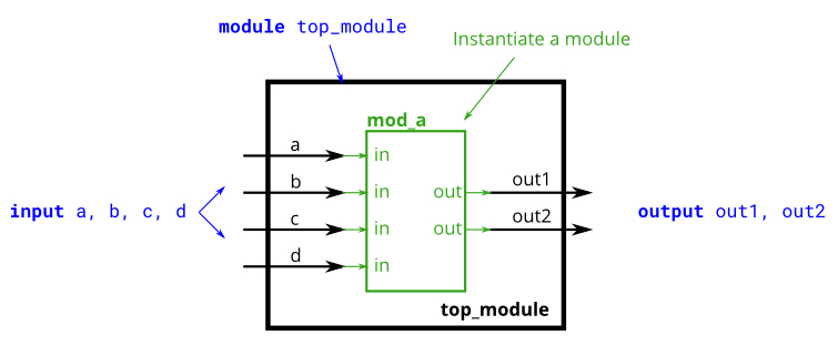
题目:完成mod_a模块的调用
题目描述:完成 mod_a 模块的调用
Solution:
1 | module top_module ( |
小贴士:模块调用有两种方式,各有优缺点:
- 按位置调用:代码简洁,但顺序不能错,适合端口很少的简单模块
- 按名称调用:代码稍显繁琐,但更稳定、可读性更好,端口顺序可以随便排
建议:只要模块端口超过3个,尽量使用按名称连接的方式!
按位置连接端口
题目描述:
已有一个名为 mod_a 的模块,它有 2 个输出和 4 个输入。您必须按位置将这 6 个端口连接到顶层模块的端口 out1、out2、a、b、c 和 d,并按顺序进行连接。
给定如下的模块:1
module mod_a ( output, output, input, input, input, input );
Solution:
1 | module top_module ( |
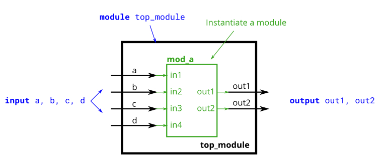
按名称连接端口
题目描述:按名称连接模块 mod_a
Solution:
1 | module top_module ( |
注意:按名称连接时,每个端口前面都要有一个点
.,然后用括号把要连接的信号括起来。这种方式虽然写起来多敲几个字,但代码的可读性和可维护性大大提高!
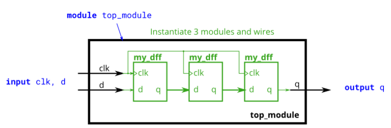
三个模块的调用
题目描述:
已有一个模块 my_dff,其中有两个输入和一个输出(D 触发器)。实例化三个 D 触发器然后将它们连接在一起,实现一个长度为 3 的移位寄存器。clk 端口需要连接到所有 my_dff 实例。
已有模块:1
module my_dff ( input clk, input d, output q );
Solution:
1 | module top_module ( |
小贴士:当内部调用多个模块时,需要定义合理的wire信号来连接这些模块。可以把这些wire想象成电路板上的铜导线,它们在各个芯片之间传递信号。
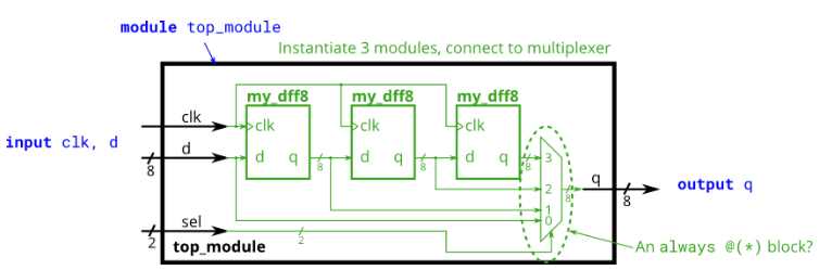
模块输入为向量
题目描述:
已有一个模块 my_dff8,它具有两个输入和一个输出(实现一组 8 位的 D 触发器)。实例化其中的三个,然后将它们连接在一起,实现一个长度为 3 的 8 位宽移位寄存器。另外,构造一个 4-1 多路选择器,根据 sel[1:0] 选择输出值。本质上,sel 选择的是延迟输入的周期。
已有模块:1
module my_dff8 ( input clk, input [7:0] d, output [7:0] q );
Solution:
1 | module top_module ( |
小贴士:组合逻辑用连续赋值(assign)或者always @(*)块都可以,哪种方便用哪种。像这种多路选择器的情况,用case语句写起来会很清晰!
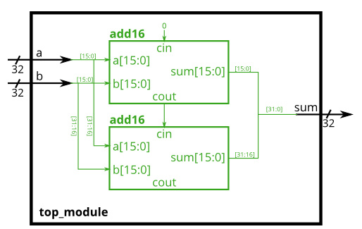
加法器模块1
题目描述:用两个带进位的16bit加法器组成一个32bit加法器。
1 | module add16 (input[15:0] a, input[15:0] b, input cin, output[15:0] sum, output cout); |
Solution:
1 | module top_module( |
小贴士:
- 注意使用拼接操作
{}来简化代码- 无用的信号接口即使作为输出也可以不连接(如高16位的cout我们没用到)
加法器模块2
题目描述:
自定义一个1bit的全加器,构成一个16bit全加器,然后用两个16bit全加器完成32bit加法模块的搭建,忽略进位。
- 定义一个1bit全加器
- 在顶层完成两个16bit全加器的调用
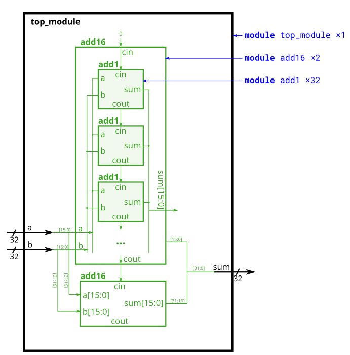
Solution:
1 | module top_module ( |
进位选择加法器
题目描述:
在这个练习中,已有和上一个练习相同的模块 add16,本题将两个16位数字相加,并生成一个输出进位和16位的和。需构造一个16位2-1多路选择器。
1 | module add16 ( input[15:0] a, input[15:0] b, input cin, output[15:0] sum, output cout ); |
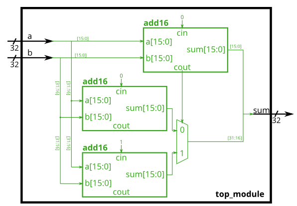
思路提示:这就是用资源换速度的典型例子!普通的行波进位加法器,高位要等低位算完才能开始算。而进位选择加法器呢?它同时计算两种情况:假设进位是0,和假设进位是1,等低位的进位真的算出来了,直接选对应的结果就行!
Solution:
1 | module top_module( |
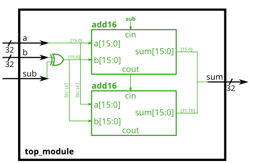
加法器→减法器
题目描述:利用sub信号和两个16bit的全加器,实现32bit的加减法运算。
对输入的sub信号进行判断:
- 如果sub=0,则输出(a + b + 0)
- 如果sub=1,则输出(a + ~b + 1)
已有模块:1
module add16 ( input[15:0] a, input[15:0] b, input cin, output[15:0] sum, output cout );
思路提示:减法可以转换成加法!还记得吗?减去一个数等于加上它的补码,而补码就是”按位取反再加1”。那怎么同时实现”按位取反”和”加1”呢?
看这里:用32位宽的XOR门,当sub=1时把b取反,同时把sub作为最低位的进位输入! 这样就一举两得了!
Solution:
1 | module top_module( |
小贴士:这个设计太巧妙了!用一个sub信号同时完成了两件事:
- 通过异或门控制b是否取反
- 作为最低位的进位输入实现”加1”
这就是硬件设计的魅力——用简单的逻辑实现复杂的功能!
入门者避坑指南
模块例化是Verilog设计中最常用的操作之一,但初学者也容易在这里踩坑。让我们看看常见的错误:
错误1:模块嵌套定义
错误表现:1
2
3
4
5
6
7
8
9
10
11
12
13
14module bad_example (
input a,
output b
);
// 错误!不能在一个模块内部定义另一个模块!
module inner_module (
input x,
output y
);
assign y = ~x;
endmodule
inner_module u1 (.x(a), .y(b));
endmodule
错误原因:
Verilog的模块是平级关系,不能嵌套定义。就像你不能把一个电路板的电路图直接画在另一个电路板的电路图里面,它们应该是分开的文件或者分开定义的。
正确做法:1
2
3
4
5
6
7
8
9
10
11
12
13
14
15// 先定义子模块
module inner_module (
input x,
output y
);
assign y = ~x;
endmodule
// 再定义顶层模块
module good_example (
input a,
output b
);
inner_module u1 (.x(a), .y(b));
endmodule
调试技巧:
- 每个模块单独定义,不要嵌套
- 可以把不同的模块放在不同的文件里,也可以放在同一个文件里(但要平级)
错误2:按位置连接时顺序错误
错误表现:1
2
3
4
5
6
7
8
9
10
11
12
13// 假设子模块的定义是这样的:
module my_dff (input clk, input d, output q);
// ...
endmodule
module bad_example (
input clk,
input [7:0] d,
output [7:0] q
);
// 错误!顺序搞反了!
my_dff u1 (d, clk, q); // 应该是 (clk, d, q)
endmodule
错误原因:
按位置连接时,顺序非常重要!必须严格按照子模块定义时的端口顺序来连接。
正确做法:1
2
3
4
5
6
7
8module good_example (
input clk,
input [7:0] d,
output [7:0] q
);
// 正确:按照定义的顺序 clk, d, q
my_dff u1 (clk, d, q);
endmodule
调试技巧:
- 记不住顺序?那就用按名称连接的方式吧!
- 如果用按位置连接,一定要把子模块的定义放在旁边对照着看
错误3:按名称连接时点号丢了
错误表现:1
2
3
4
5
6
7
8
9
10module bad_example (
input a,
output b
);
// 错误!端口名前面少了点号!
my_module u1 (
in(a), // 应该是 .in(a)
out(b) // 应该是 .out(b)
);
endmodule
错误原因:
按名称连接的语法是.端口名(信号名),点号.不能丢!
正确做法:1
2
3
4
5
6
7
8
9
10module good_example (
input a,
output b
);
// 正确:每个端口前面都有点号
my_module u1 (
.in(a),
.out(b)
);
endmodule
调试技巧:
- 按名称连接的口诀:先有点,后有名,括号里面是信号名
错误4:连接信号的位宽不匹配
错误表现:1
2
3
4
5
6
7
8
9
10module bad_example (
input [3:0] a, // 4位
output [3:0] b
);
// 假设子模块的端口是8位的
my_module u1 (
.in(a), // 错误!in是8位,a是4位,位宽不匹配
.out(b)
);
endmodule
错误原因:
连接信号时,位宽要匹配,否则可能会产生意想不到的结果(如高位被截断或补零)。
正确做法:1
2
3
4
5
6
7
8
9
10
11
12
13
14
15
16
17
18module good_example (
input [3:0] a,
output [3:0] b
);
wire [7:0] temp_in;
wire [7:0] temp_out;
// 位宽匹配:把4位扩展到8位(高位补零)
assign temp_in = {4'd0, a};
my_module u1 (
.in(temp_in),
.out(temp_out)
);
// 取低4位
assign b = temp_out[3:0];
endmodule
调试技巧:
- 大多数综合工具会对位宽不匹配发出警告,注意看警告信息
- 可以用
$bits()系统函数检查信号的位宽
错误5:忘记定义中间连接信号
错误表现:1
2
3
4
5
6
7
8module bad_example (
input a,
output c
);
// 错误!temp信号没有定义!
sub_module1 u1 (.in(a), .out(temp));
sub_module2 u2 (.in(temp), .out(c));
endmodule
错误原因:
连接多个模块的中间信号必须显式定义为wire类型。
正确做法:1
2
3
4
5
6
7
8
9
10module good_example (
input a,
output c
);
// 正确:先定义中间信号
wire temp;
sub_module1 u1 (.in(a), .out(temp));
sub_module2 u2 (.in(temp), .out(c));
endmodule
调试技巧:
- 画个电路图,把需要的连接线都标出来,然后对应定义wire
本章小结
这一章我们学习了模块的例化与调用,这是Verilog设计的核心技能之一:
- 模块的概念:把功能封装起来,对外只留接口,就像电路板一样
- 两种连接方式:
- 按位置连接:简洁但顺序不能错
- 按名称连接:稍繁琐但更稳定、可读性更好(推荐)
- 层次化设计:用多个小模块搭建大系统,这就是”对着电路图写HDL”
- 实用技巧:
- 多个模块连接时,需要定义中间wire信号
- 向量作为端口时,连接方式和单个信号一样
- 可以用拼接操作来简化代码
- 未使用的输出端口可以不连接
模块例化让我们能够构建复杂的数字系统,从小的加法器到完整的处理器,都是这样一层层搭建起来的!
 微信
微信 支付宝
支付宝